Co-Portfolio Manager


• インサイト
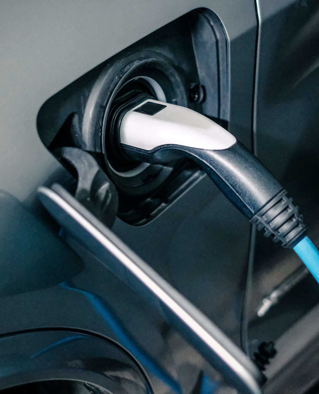
Why the future of chips depends on water
Accelerating AI and digitalization trends are pushing up the demand for chips and water. To hedge against potential shortages, chipmakers and municipalities alike are investing in utility-scale water recycling solutions, creating a groundswell of growth for companies along the water value chain.
執筆者

主なキーワード
まとめ
- Semiconductor manufacturing is a water-intensive process
- Advanced chips, digitization, and climate change are pushing demand higher
- Chipmakers are investing in utility-scale water treatment solutions
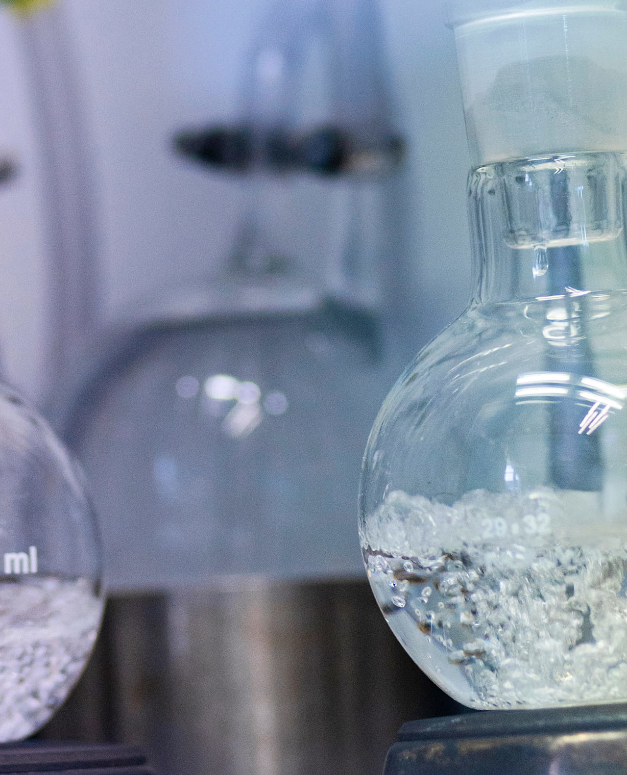
Semiconductor manufacturing is not only energy-intensive, but also extraordinarily water-intensive. The fabrication plants (or ‘fabs’) that produce the chips that underpin AI, data centers and modern electronics rely heavily on ultra-pure water (UPW) for rinsing and cleaning as chips are etched on silicon wafers. High-performance chips used in AI models, data center infrastructure and premium smart phones require even more water, pushing the industry’s water demands even higher as they expand (see Figure 1).
Unsurprisingly, industry estimates suggest that a single fab can uses roughly 20-38 million liters of water a day – enough to rival the daily consumption of a small city.1 Large multi-fab sites can exceed this range, particular in hot, water-stressed regions.2 Taiwan’s chipmaking titan, TSMC, consumed 101 billion liters of water in 2023 alone, with consumption levels rising as next-gen nodes add more layers of circuitry. 3 Those figures rise precipitously when aggregated across the entire industry.
Figure 1 – Water intensity of chips continues to rise

Average water intensity per chip, Source: Xylem, GWI, 2026.
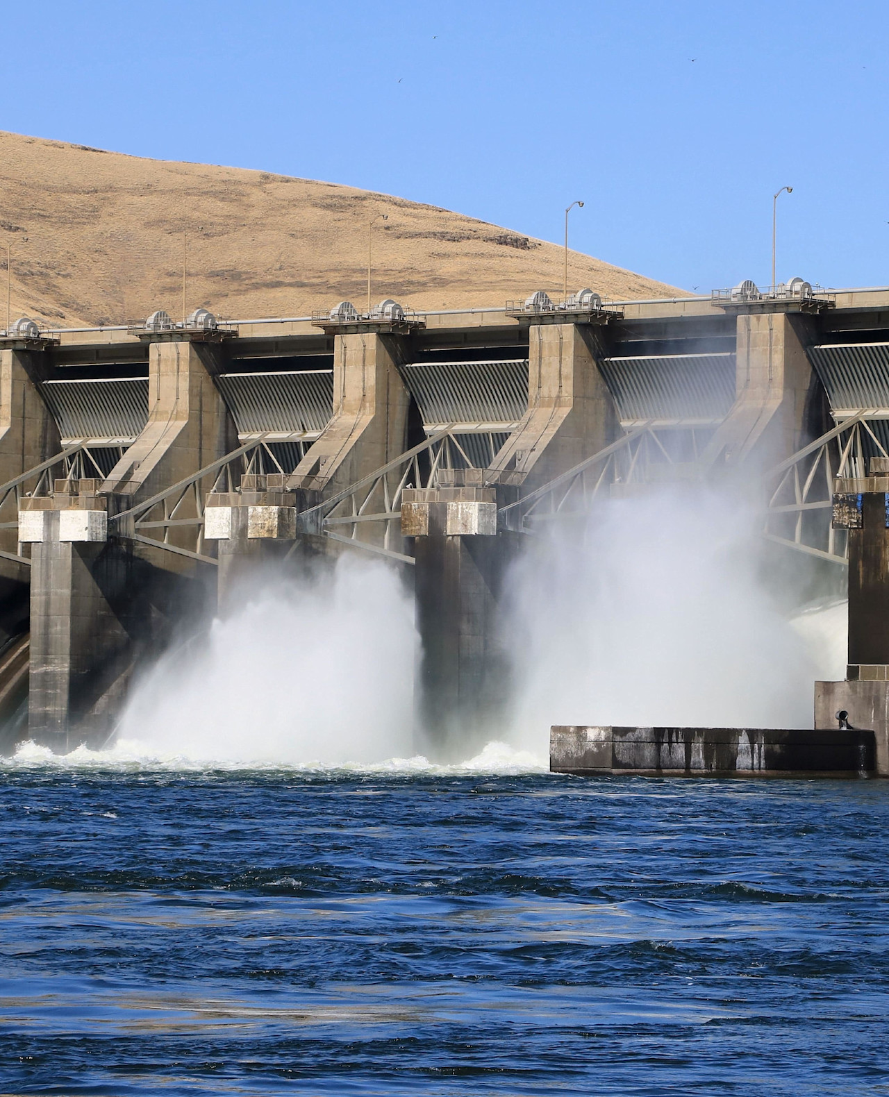
Recycling and reclaiming are mission critical
Of course, not all water used in a fab must be ultra-pure. Chip manufacturing relies on multiple grades of water quality for different operations. To reduce external withdrawals from municipal utilities and local watersheds, fabs must reuse water in securely managed loops. For example, UPW, once used, is recycled for use in lower-grade processes such as cooling towers and for wet scrubbing (treating fab exhaust gases). Fabs also ensure that water discharged externally meets strict EPA standards, which are getting more stringent with recent regulations on PFAS and other chemical toxins.4 Recycling at this intensity and scale requires a full suite of water technologies including: advanced treatment systems to remove particles, metals and other residue; real-time monitoring tools that verify water purity at multiple stages; and special piping to distribute flows whose coatings don’t leach and corrode water streams.
Figure 2 – Semiconductor manufacturing water cycle

Source: Robeco, 2026. Logos sourced from company websites or publicly available sources. The companies/securities are not necessarily held by a strategy/fund nor is future inclusion guaranteed. No inference can be made on the future development of the company. This is not a buy, sell, or hold recommendation.
AI and data center growth
In the US, fab growth continues to benefit from the US CHIPS Act which committed USD 39 billion in incentives to reshore and boost semiconductor and advanced manufacturing capacity through 2032.5
Figure 3 – Water demand growth in chip manufacturing and related AI industries

Source: Xylem, GWI, 2026.
Investment and growth in AI and data centers are not limited to the US. The European Union unveiled the European CHIPS Act, China initiated the third phase of its Integrated Circuit (IC) Industry Investment Fund, and various other incentive programs have emerged in Taiwan, South Korea, Japan, India, and around the world.6 In addition to governments, projected private sector capex totals around USD 2.3 trillion from 2024-2032.7 According to most assessments, the semiconductor industry was valued in the range of USD 630 billion to USD 680 billion in 2024 and is expected to reach over USD 1 trillion by 2030, largely fueled by the growth of AI and data centers.8
Fab location – intensifying the water problem
To make matters worse, semiconductor manufacturing is increasingly concentrated in regions already facing water scarcity. In the US, planned and existing fabs are located in areas that face medium to severe water stress.9 Globally, critical hubs in Taiwan, South Korea, Singapore, and northern China face similar constraints. A recent analysis found that around 40% of existing semiconductor fabs – and more than 40% of new fabs announced since 2021 – are located in areas projected to face high or extremely high water stress by 2030. 10
This presents a real operational risk to one of the world’s most strategically important supply chains. Taiwan’s 2021 drought illustrated how water scarcity can disrupt production and force emergency measures (including trucked-in water deliveries). To reduce risks, best-in-class fabs are targeting >70% water recycling and will need even higher levels to operate in drought prone regions by 2030-2035.11
Rising demand requires more utility-scale infrastructure
To combat growing water challenges, leading chip manufacturers are investing heavily in onsite treatment, recycling, and closed-loop water systems. In late 2025, TSMC began construction on a 15-acre industrial water reclamation plant designed to recycle up to 90% of wastewater from its fabs in Arizona’s Silicon Valley.12
Intel is also spending hundreds of millions on water infrastructure at its Arizona-based, both on-site as well as on municipal-owned infrastructure. It recently partnered with the city of Chandler (a Phoenix suburb) to construct the Ocotillo Brine Reduction Facility – an off-site plant that will add 11 million liters of treatment capacity to Intel’s 12-acre on-site treatment plant.1314 Similarly, Samsung is partnering with South Korea’s Gyeonggi Province to construct treatment facilities that would enable it use municipal wastewater from five cities for its chipmaking facilities in the area by 2029.15
In Germany’s Silicon Saxony, it’s the local authorities who are doing the investing. The EUR 320 million project will ensure uninterrupted supplies of water to the region’s booming semiconductor cluster, whose water demand is expected to significantly increase in the decades ahead.16 Taiwan’s government is also building a major seawater desalination plant to secure water supplies for Hsinchu Technology Park, a major chipmaking hub which includes TSMC fabs. The plant is expected to be finished in 2028 at a cost of EUR 508 million. Hsinchu is part of a national water strategy that will see eight desalination plants constructed to support advanced semiconducting manufacturing.17
New waves of growth for water companies
This multi-year expansion of fabs translates into demand across multiple segments of the industrial water value chain. Semiconductor water systems rely on complex networks of treatment, purification, cooling, monitoring, and piping and distribution in order to deliver ultrapure water while safely managing contaminated wastewater streams. Large treatment and reclamation plants require advanced membranes, reverse osmosis, and ion exchange technologies to remove particles and dissolved contaminants.
Within the fab, additional purification stages produce UPW for wafer cleaning, while separate systems manage cooling water used to dissipate heat in facility operations. Continuous monitoring systems track water quality, while specialized pumps, valves, and piping move chemically complex water safely through the facility. As AI-driven chip production and data infrastructure expand globally, demand for water solutions is expected to grow across the entire water value chain.
Footnotes
1 iScience, Sept 2025, https://pmc.ncbi.nlm.nih.gov/articles/PMC12510042; Semiconductor Digest, September 2025, https://www.semiconductor-digest.com/creating-semiconductor-manufacturing-solutions-with-sustainability-in-mind
2 August 2025, https://semiengineering.com/how-semiconductor-fabs-use-water/
3 https://www.idtechex.com/en/research-article/water-usage-in-semiconductor-manufacturing-to-double-by-2035/32746
4 Manufacturing dive, semiconductor industry faces water, sustainability challenges...
5 America projected to triple semiconductor manufacturing capacity by 2032. Semiconductor Industry Association, May 2024.
6 America projected to triple semiconductor manufacturing capacity by 2032. Semiconductor Industry Association, May 2024.
7 Emerging resilience in the semiconductor supply chain. Semiconductor Industry Association, May 2024
8 https://www.mckinsey.com/industries/semiconductors/our-insights/hiding-in-plain-sight-the-underestimated-size-of-the-semiconductor-industry
9 Arizona, Texas, New Mexico, California, Utah, Idaho, and Oregon https://www.ncei.noaa.gov/access/monitoring/monthly-report/drought/202513
10 TNFD, Nature-related issues in the technology sector. February 2026.
11 https://energy-solutions.co/articles/sub/semiconductor-foundries-managing-extreme-power-density-water-risks
12 TSMC breaks ground on water reclamation project. Data Center Dynamics, September 2025.
13 Intel Newsroom, Intel’s Ocotillo Campus honored for water stewardship, July 2023.
14 Inside Intel’s new Arizona fab, CNBC, December 2025.
15 Samsung Semiconductor Newsroom, Samsung signs MOU with MoE and local governments. December 2024.
16 New river waterworks on the Elbe. Silicon Saxony, September 2023.; TSMC: ESMC breaks ground on Dresden fab, August 2024.
17 CTCI Group Newsletter, May 2025. Suez Press Release, June 2024.
サステナビリティに関する最新のインサイトを把握
ロベコのニュースレター(英文)に登録し、サステナブル投資の最新動向を探求しましょう。
重要事項
当資料は情報提供を目的として、ロベコ・ジャパン株式会社(以下「当社」)が独自に作成、または当社のグループ会社(Robeco Institutional Asset Management B.V.およびその関連会社を含む)から提供された資料を当社が編集・翻訳したものです。資料中の個別の金融商品の売買の勧誘や推奨等を目的とするものではありません。記載された情報は十分信頼できるものであると考えておりますが、その正確性、完全性を保証するものではありません。意見や見通しはあくまで作成日における弊社の判断に基づくものであり、今後予告なしに変更されることがあります。運用状況、市場動向、意見等は、過去の一時点あるいは過去の一定期間についてのものであり、過去の実績は将来の運用成果を保証または示唆するものではありません。また、記載された投資方針・戦略等は全ての投資家の皆様に適合するとは限りません。当資料は法律、税務、会計面での助言の提供を意図するものではありません。 ご契約に際しては、必要に応じ専門家にご相談の上、最終的なご判断はお客様ご自身でなさるようお願い致します。 運用を行う資産の評価額は、組入有価証券等の価格、金融市場の相場や金利等の変動、及び組入有価証券の発行体の財務状況による信用力等の影響を受けて変動します。また、外貨建資産に投資する場合は為替変動の影響も受けます。運用によって生じた損益は、全て投資家の皆様に帰属します。したがって投資元本や一定の運用成果が保証されているものではなく、投資元本を上回る損失を被ることがあります。弊社が行う金融商品取引業に係る手数料または報酬は、締結される契約の種類や契約資産額により異なるため、当資料において記載せず別途ご提示させて頂く場合があります。具体的な手数料または報酬の金額・計算方法につきましては弊社担当者へお問合せください。 当資料及び記載されている情報、商品に関する権利は弊社に帰属します。したがって、弊社の書面による同意なくしてその全部もしくは一部を複製またはその他の方法で配布することはご遠慮ください。 商号等: ロベコ・ジャパン株式会社 金融商品取引業者 関東財務局長(金商)第2780号 加入協会: 一般社団法人 資産運用業協会